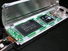
Universal Flash Storage (UFS) is a common flash storage specification for digital cameras, mobile phones and consumer electronic devices.[1][2] This could bring higher data transfer speed and increased reliability in flash memory storage, thus reducing market confusion and the varying number of adapters for different number of cards.[3]
The proposed specification is supported by leading firms in the consumer electronics industry such as Nokia, Sony Ericsson, Texas Instruments, STMicroelectronics, Samsung and Micron.[4] The electrical interface for UFS uses the M-PHY.,[5] developed by the MIPI Alliance.[6] organization. This offers the possibility of higher speed, ease of integration into embedded applications, and lower power consumption compared to SD cards.[7]
The standard is currently being constructed by the JEDEC Solid State Technology Association.[8]
---------------------------------------
| Computer memory types |
|---|
| Volatile |
| RAM |
| In development |
| Historical |
|
| Non-volatile |
| ROM |
| NVRAM |
|
| Early stage NVRAM |
| Mechanical |
| In development |
| Historical |
|
Flash memory was developed from EEPROM (electrically erasable programmable read-only memory). There are two main types of flash memory, which are named after the NAND and NOR logic gates. The internal characteristics of the individual flash memory cells exhibit characteristics similar to those of the corresponding gates.
Whereas EPROMs had to be completely erased before being rewritten, NAND type flash memory may be written and read in blocks (or pages) which are generally much smaller than the entire device. The NOR type allows a single machine word (byte) to be written or read independently.
The NAND type is primarily used in main memory, memory cards, USB flash drives, solid-state drives, and similar products, for general storage and transfer of data. The NOR type, which allows true random access and therefore direct code execution, is used as a replacement for the older EPROM and as an alternative to certain kinds of ROM applications, whereas NOR flash memory may emulate ROM primarily at the machine code level; many digital designs need ROM (or PLA) structures for other uses, often at significantly higher speeds than (economical) flash memory may achieve. NAND or NOR flash memory is also often used to store configuration data in numerous digital products, a task previously made possible by EEPROMs or battery-powered static RAM.
Example applications of both types of flash memory include personal computers, PDAs, digital audio players, digital cameras, mobile phones, synthesizers, video games, scientific instrumentation, industrial robotics, medical electronics, and so on. In addition to being non-volatile, flash memory offers fast read access times, as fast as dynamic RAM, although not as fast as static RAM or ROM. Its mechanical shock resistance helps explain its popularity over hard disks in portable devices, as does its high durability, being able to withstand high pressure, temperature, immersion in water, etc.[1]
Although flash memory is technically a type of EEPROM, the term "EEPROM" is generally used to refer specifically to non-flash EEPROM which is erasable in small blocks, typically bytes. Because erase cycles are slow, the large block sizes used in flash memory erasing give it a significant speed advantage over old-style EEPROM when writing large amounts of data. Flash memory now costs far less than byte-programmable EEPROM and has become the dominant memory type wherever a significant amount of non-volatile, solid state storage is needed.
History
Flash memory (both NOR and NAND types) was invented by Dr. Fujio Masuoka while working for Toshiba circa 1980.[2][3] According to Toshiba, the name "flash" was suggested by Masuoka's colleague, Shōji Ariizumi, because the erasure process of the memory contents reminded him of the flash of a camera.[citation needed] Masuoka and colleagues presented the invention at the IEEE 1984 International Electron Devices Meeting (IEDM) held in San Francisco.[4]Intel Corporation saw the massive potential of the invention and introduced the first commercial NOR type flash chip in 1988.[5] NOR-based flash has long erase and write times, but provides full address and data buses, allowing random access to any memory location. This makes it a suitable replacement for older read-only memory (ROM) chips, which are used to store program code that rarely needs to be updated, such as a computer's BIOS or the firmware of set-top boxes. Its endurance may be from as little as 100 erase cycles for an on-chip flash memory,[6] to a more typical 10,000 or 100,000 erase cycles, up to 1,000,000 erase cycles.[7] NOR-based flash was the basis of early flash-based removable media; CompactFlash was originally based on it, though later cards moved to less expensive NAND flash.


 LibreOffice
 Firefox
No comments:
Post a Comment